Confocal Microscopy: Difference between revisions
| (204 intermediate revisions by 2 users not shown) | |||
| Line 1: | Line 1: | ||
==Introduction== | ==Introduction== | ||
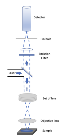
[[File: Fig 2 .png|x450px|right|thumb|Figure 1. Schematic of confocal microscopy]] | |||
A [https://en.wikipedia.org/wiki/Confocal_microscopy Confocal Microscopy] is an optical imaging technique for increasing optical resolution and contrast of a micrograph. It uses pinhole to block out all out of focus light to enhance optical resolution, very different from traditional wide-field fluorescence microscopes. To offset the block of out of focus lights, the light intensity is detected by a photomultiplier tube or avalanche photodiode, which transforms the light signal into an electrical one. We will try to build a Setup like this to enhance optical resolution and maybe get profile information about the sample. | A [https://en.wikipedia.org/wiki/Confocal_microscopy Confocal Microscopy] is an optical imaging technique for increasing optical resolution and contrast of a micrograph. It uses pinhole to block out all out of focus light to enhance optical resolution, very different from traditional wide-field fluorescence microscopes. To offset the block of out of focus lights, the light intensity is detected by a photomultiplier tube or avalanche photodiode, which transforms the light signal into an electrical one. We will try to build a Setup like this to enhance optical resolution and maybe get profile information about the sample. | ||
| Line 9: | Line 9: | ||
==Principles of confocal microscopy== | ==Principles of confocal microscopy== | ||
The method of image formation in a confocal microscope is fundamentally different from that in a conventional [https://en.wikipedia.org/wiki/Fluorescence_microscope fluorescence microscope ], where the entire specimen is subjected to intense illumination from an incoherent | The method of image formation in a confocal microscope is fundamentally different from that in a conventional [https://en.wikipedia.org/wiki/Fluorescence_microscope fluorescence microscope ], where the entire specimen is subjected to intense illumination from an incoherent lamp, and resulting image of secondary fluorescence emission can be viewed directly by eye or detector. This usually requires a thin, relatively transparent, sample but often results in out-of-focus blur that reduces resolution and specimen contrast. In contrast, the illumination in a confocal microscope is achieved by scanning focused beam from laser and across the specimen. | ||
The confocal principle is diagrammatically presented in Figure 1. Coherent light emitted by the laser system (excitation source) pass through a low-pass filter that is situated in a conjugate plane (confocal) with a scanning point on the specimen and a pinhole aperture positioned in front of the detector (Si PIN photodiode). As the laser is reflected by a dichromatic mirror and scanned across the specimen in a defined focal plane, secondary fluorescence emitted from points on the specimen pass back through the dichromatic mirror and are focused as a confocal point at the pinhole aperture. | The confocal principle is diagrammatically presented in Figure 1. Coherent light emitted by the laser system (excitation source) pass through a low-pass filter that is situated in a conjugate plane (confocal) with a scanning point on the specimen and a pinhole aperture positioned in front of the detector (Si PIN photodiode). As the laser is reflected by a dichromatic mirror and scanned across the specimen in a defined focal plane, secondary fluorescence emitted from points on the specimen pass back through the dichromatic mirror and are focused as a confocal point at the pinhole aperture. | ||
| Line 19: | Line 18: | ||
[[File:Optical_path_of_confocal_microscopy.png|x250px|center|thumb|Figure 2. Optical path diagram of confocal microscope]] | [[File:Optical_path_of_confocal_microscopy.png|x250px|center|thumb|Figure 2. Optical path diagram of confocal microscope]] | ||
=== | ===XYZ piezo scanner=== | ||
[[File:Fig 5.png|x300px|center|thumb|Figure 3. Modified micro PI stage controller.]] | |||
===Si PIN | Piezo scanners are used for fast, high precision motion in one or more axes. In our project, we combine the micro PI stage controller with a moving stage on x-axis to realise three dimensional piezo scanning in our confocal microscopy. | ||
[[File:Fig 3.png| | |||
High-speed Si PIN photodiodes are designed for visible to near infrared light detection for they can efficiently convert light into an electrical current. The current is generated when photons are absorbed in the photodiode. These photodiodes provide wide-band characteristics at a low bias, making them suitable for optical communications. In this project, we choose S5973 series with a mini-lens type (S5973-01) that can be efficiently coupled with an optical fiber and a violet sensitivity enhanced type (S5973-02) ideal for violet laser detection. | ===Si PIN Photodiode=== | ||
[[File:Fig 3.png|x400px|center|thumb|Figure 4. High-speed photodiode.]] | |||
High-speed Si PIN photodiodes are designed for visible to near infrared light detection for they can efficiently convert light into an electrical current. The current is generated when photons are absorbed in the photodiode. These photodiodes provide wide-band characteristics at a low bias, making them suitable for optical communications. In this project, we choose S5973 series with a mini-lens type (S5973-01) that can be efficiently coupled with an optical fiber and a violet sensitivity enhanced type (S5973-02) ideal for violet laser detection. By combining the PIN photodiode with our adjustable optical pinhole, we get the receiving end of our confocal microscopy | |||
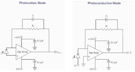
Photodiode has two working modes: solar cell mode (photovoltaic mode) and photoconductive mode. Solar cell mode is otherwise called as Zero Bias Mode. When a photodiode operates in low frequency applications and ultra-level light applications, this mode is preferred. When photodiode is irradiated by a flash of light, voltage is produced. The voltage produced will have a very small dynamic range and it has a non-linear characteristic. When photodiode is configured with OP-AMP in this mode, there will be a very less variation with temperature. (sketch diagram see link below). | |||
In the photoconductive mode, photodiode will act in reverse biased condition. Cathode will be positive and anode will be negative. When the reverse voltage increases, the width of the depletion layer also increases. Due to this the response time and junction capacitance will be reduced. Comparatively this mode of operation is fast and produces electronic noise. | |||
[[File:Fig 12.png|x300px|center|thumb|Figure 5. The diagram of circuit for photovoltaic mode and photoconductive mode.]] | |||
===Arduino Uno=== | |||
[[File:Fig 10.png|x300px|center|thumb|Figure 6. Detector of the confocal microscopy (Arduino UNO).]] | |||
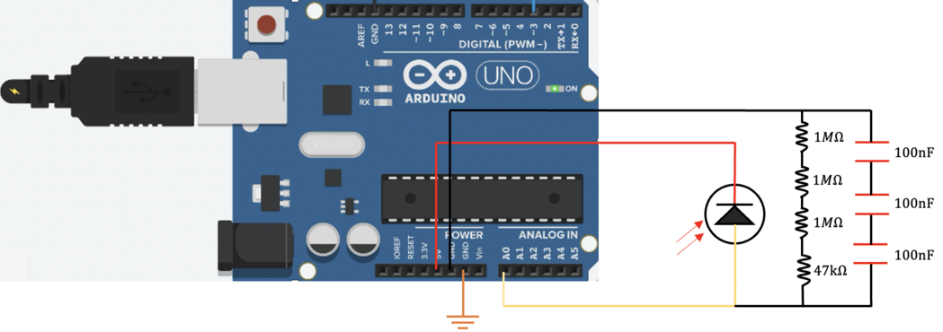
In our confocal set up, we use a 5V DC supply to inverse biase ( connect to the cathode of )the photodiode and operate it under a photoconductive mode. Some resistors are connect between photodiode anode side and ground (GND) to amplify the signal from the photodiode and convert the photo current to an readable voltage. A 47K Ohm is first adopted in the circuit, later found out that this resistor is not big enough, then we added three more 1M Ohm resistors (3.047M Ohm in total). Then three 100 nF capacitors in series (100/3 nF in total )were connected btw photodiode anode side and ground (GND) to filter out the high frequency noises of photocurrent. Finally, We use an arduino analog input pin A0 to read out the voltage at the anode side of photodiode. | |||
Also, in our photoconductive mode, we didn't use an OP-AMP, but connecting our voltage metter directly with our photodiode's anode. | |||
[[File:Fig 11.png|x370px|center|thumb|Figure 7. A diagram of the signal processing circuit using with Arduino UNO).]] | |||
====Code==== | |||
* Here is an Arduino sketch to read the output voltage of the photodiode detectors. | |||
The output pin of the circuit is connected to analog pin 0 of the Arduino. | |||
The data are read every 0.025 second in this example. | |||
However, you can change the sampling rate by simply changing the argument of the delay() statement. * | |||
#define inPin0 0 | |||
void setup(void) { | |||
Serial.begin(9600); | |||
Serial.println(); | |||
} | |||
void loop(void) { | |||
float pinRead0 = analogRead(inPin0); | |||
Serial.println(pinRead0); | |||
/* the minimum delay allowed is about 20, correspond | |||
is about 20ms */} | |||
delay(25); | |||
} | |||
==Experimental process== | ==Experimental process== | ||
===Laser calibration=== | ===Laser calibration=== | ||
[[File:Fig | [[File:Fig 8.png|x400px|center|thumb|Figure 8. Laser calibration process.]] | ||
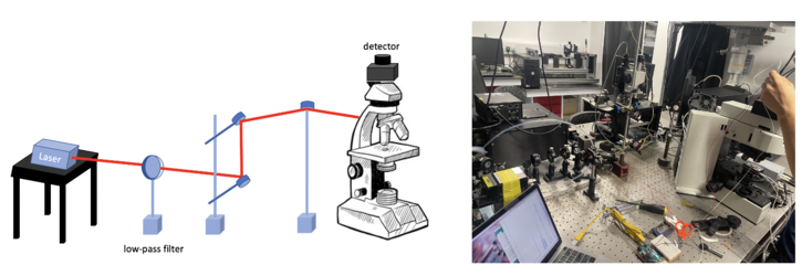
To realise the focus both on the focal plane of specimen and pinhole aperture, we built the set up shown in Figure.6. After the adjustment, we fix the height of the detector. | |||
===Measurement of coin sample=== | |||
====Step 1==== | |||
Firstly, we managed to find the focus point within the region of 400um along z axis for each point on our coin by y-z micro PI stage controller. | |||
====Step 2==== | |||
After that, we translated 100um on x-axis per step to find next focus point on z direction. We moved 10 steps in total so that the total distance along y-axis is 1000um. | |||
====Step 3==== | |||
At last, we moved 100um on x-axis through tuning the spiral and measured the final set of data. | |||
=Experimental results= | |||
We tried to scan a 1mm*1mm area on the coin, and the area we focus is basically ‘E’ of word CENTS on a 50 cents Singapore dollar. Here are the scanning parameters of our experiment. | |||
[[File:Fig_a.png|x100px|center|thumb|Table 1. Scanning parameters]] | |||
We used two piezo stage to move along y and z axis automatically, and a spiral micrometer to move the stage along x axis. Here we want to scan 10 points along x axis, 10 points along y axis and 80 points along z axis. Here is how we scan our sample: start from (x,y,z) the receiver will automatically scan 80 points when piezo moves upward along z axis (for scanning of each point piezo will take for about 85ms) and reach point (x,y,z+400), it will go pass the focused point of this certain (x,y) along the scanning of z axis, then piezo will move to point (x,y+100,z+400) and hold there for 5 seconds, then it will movie downward and reach point (x,y+100,z), it will pass through the focused point of this (x,y+400), and after that, it will move to point (x,y+200,z) and hold there still for 5 seconds. After 5 iterations of this, we will reach point (x,y+1000,z) and then we will use micrometer move the stage manually to point (x+100, y+1000,z) and repeat another 5 iterations, after moving 9 times we will reach point (x+1000, y+1000,z) finally. Figure 9 is the typical scanning pattern of two points (x,y,z+400) and (x,y+100,z+400), so we can find two corresponding maximum A&B in the plot, C is the point when piezo starts to hold still for 5 seconds. | |||
By getting length AC and BC, we can calculate height and intensity information about each (x, y). I use MATLAB function NF.m to filter noise and Figure.9 illustrates the filtered data. Here is how we convert AC and BC to height Information. AC and BC are actually number of data points (in the spacing). We know that Arduino will sent one data to MATLAB every 25ms, so AC and BC can be converted to time. Then we know that the scanning speed of piezo stage along z axis is about 59um/s (micrometer per second), hence AC and BC can be converted to distance. Here AC and BC indicates the distance of two maximum (focused) points A and B to the upper surface, using total height 400um to subtract AC, BC will give us the height of A,B (to the lower surface). | |||
[[File:Fig b.png|x400px|center|thumb|Figure 9. Typical scanning pattern of two points (x,y,z+400) and (x,y+100,z+400)]] | |||
Dataphones are used to analyse the final intensity and height data. The intensity data of our sample are shown in Table 2. | |||
[[File:Fig_c.png|x400px|center|thumb|Table 2. Intensity data.]] | |||
The height data of our sample are shown in Table 3. | |||
[[File:Fig_d.png|x375px|center|thumb|Table 3. Height data.]] | |||
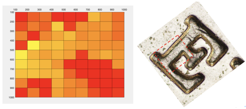
After that, we used the DrawSurf.m to draw Intensity data as illustrated in Figure 10. By comparing this result with the original "E" picture under an Optical microscope, we can find indeed this result looks like a letter "E". | |||
[[File:Fig_e.png|x405px|center|thumb|Figure 10. The original letter "E" under Optical Microscope and the results of DarwSurf.m]] | |||
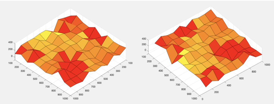
Besides, we also used the DrawTopo.m to draw Intensity data and Height data as illustrated in Figure.11. Height of the brighter orange region is bigger than the darker red region. By comparing this result with the original "E" picture under an Optical microscope, we can find indeed this result also looks like a letter "E". | |||
[[File:Fig_f.png|x350px|center|thumb|Figure 11.The original letter "E" under Optical Microscope and the results of DarwTopo.m]] | |||
The final 3D results are shown in Figure 12. From that, it can be find that we have realised the three-dimensional imaging by confocal microscope. | |||
[[File:Fig g.png|x350px|center|thumb|Figure 12. 3D results of DrawTopo.m]] | |||
===Data Processing=== | |||
====Matlab Code==== | |||
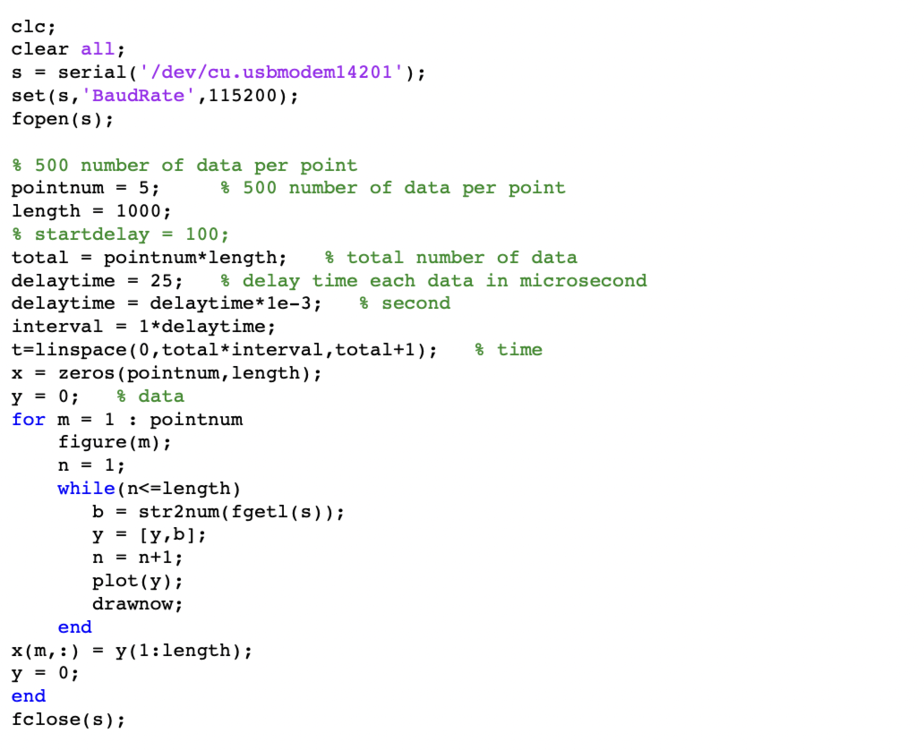
This SerialCom_Read.m program will build up serial communication between MATLAB and Arduino Board. The Arduino Board will read data from Photodiode and send data to MATLAB with a baud rate of 115200 (maximum of 115200 bits per second). | |||
[[File:Fig n.png|x750px|center|thumb]] | |||
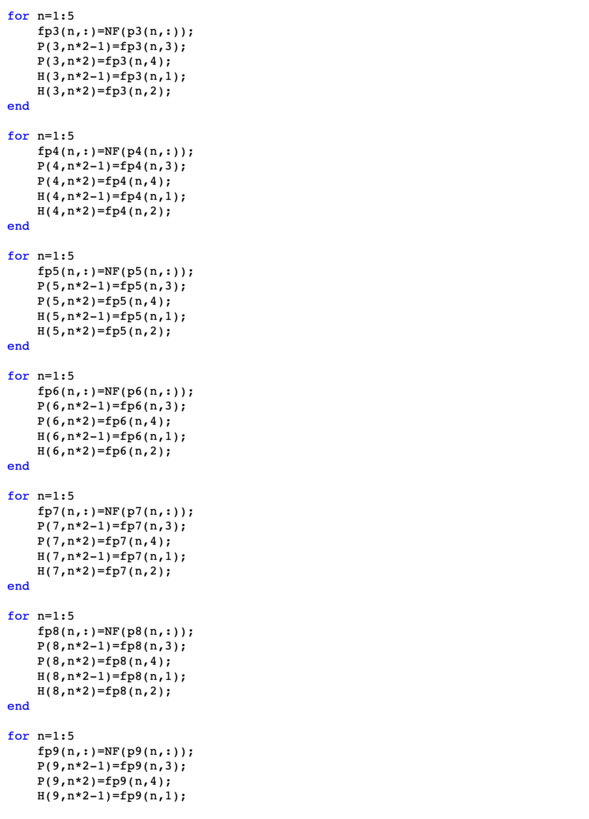
This program will process data and calculate the Height and Intensity Matrix | |||
[[File:Fig_h.png|x800px|center|thumb]] | |||
[[File:Fig i.png|x820px|center|thumb]] | |||
[[File:Fig_j.png|x220px|center|thumb]] | |||
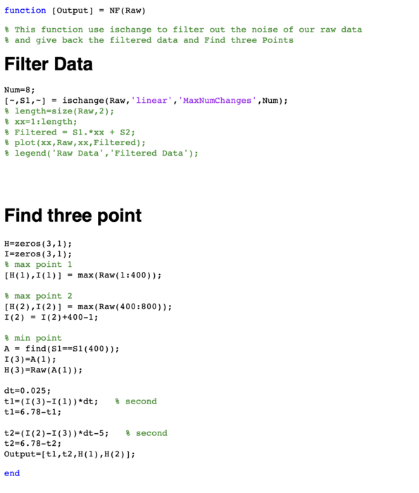
This program will filter out Noise and calculate AC, BC | |||
[[File:Fig k.png|x700px|center|thumb]] | |||
This program will draw 2D image of the scanned area | |||
[[File:Fig_l.png|x140px|center|thumb]] | |||
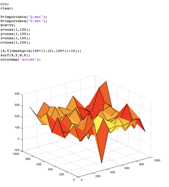
This program will draw 3D profile of the scanned sample area | |||
[[File:Fig m.png|x650px|center|thumb]] | |||
==Discussion== | |||
In this project, we have successfully construct the confocal microscopy and further applicate that to realise the three-dimensional imaging of coin. However, some limitation should be noted. First, the long scanning time limited the scanning size of our samples, which means that we still need to figure out the program optimisation to realise the large-area scanning with shorter time. Moreover, our optical devices may juggle during the experimental process for they are not fully fixed on the console, which may introduce the noise and instrumental error to our system. That should be carefully considered if we want to get a better results from this system. | |||
==Remained Problems and Future Works== | |||
We have came across many problems in setting up this confocal microscopy. We resolved most of them, yet there are still a few remained. | |||
To start with, for the XYZ scanner, we only have two piezo stages which can only provide automatic scanning on two directions, on the x direction we adopted a spiral micrometer which still requires manual adjustment. If automatic scanning on x direction is also achieved using an optical scanning stage, the efficiency of our laser scanning confocal microscope will be increased substantially. | |||
Another problem is the receiving optical path which is required to refocus the reflected laser light on a spot with a certain height. However, this height is not adjustable in our setup which means that we can only change the position of our pinhole and photodiode. If height of the focused laser spot is adjustable, we can fix the pinhole and adjust the receiving optical path to refocus the beam onto the pinhole. | |||
The Signal to Noise Ratio of our confocal microscopy is too low for a precision measurement system, with capacitors added to filter out the high frequency noise, we can only achieve SNR (20Lg(Vs/Vn)) of about 40dB. In order to achieve a higher SNR, we need to redesign photodiode's signal amplify circuit. | |||
The piezo stage scanning and photodiode data collection is not synchronized in our system. We use different programs to control the scanning and data collection, so synchronizing them is barely possible. In order to help data receiving end distinguish different scan points and be aware of the change of location, the piezo will hold for 5 seconds after scan along z axis of each (x,y). If data collection end could be informed instantaneously when piezo stage moves its position, efficiency of the scanning could enhanced. | |||
The last problem is that our system can't achieve quite accurate height information about the scanned area, so 3D profiling remains a problem. Some factors might be responsible for the inaccurate height information in the coin scanning. For instance, we did a 1mm*1mm scan with a resolution of only 10*10, which is quite low to depict more detailed surface information, however, higher resolution means more time consuming. Another possible factor is the imperfection in our data processing program, this might cause us found a wrong maximum point and thus gave us a wrong height of the focused point. | |||
Except solving those problems mentioned above and increase the efficiency and precision of our confocal microscopy, there are still some functions we wish to achieve on our Laser Scanning Setup. We wish to achieving the detection of fluorescence other than reflected light, we will need an optical filter to filter out the reflected light and a much more sensitive sensor to detect and collect the fluorescence light. Longer scanning time each point might be able to offset the requirement on sensor, yet this will also decrease the efficiency of the scanning system. With the fluorescence detection ability, we will try to detect some living creatures based on this system. | |||
==Lab Location== | ==Lab Location== | ||
S12-01-10/11 Nanomaterials Research Lab | S12-01-10/11 Nanomaterials Research Lab | ||
Latest revision as of 02:26, 7 May 2022
Introduction
A Confocal Microscopy is an optical imaging technique for increasing optical resolution and contrast of a micrograph. It uses pinhole to block out all out of focus light to enhance optical resolution, very different from traditional wide-field fluorescence microscopes. To offset the block of out of focus lights, the light intensity is detected by a photomultiplier tube or avalanche photodiode, which transforms the light signal into an electrical one. We will try to build a Setup like this to enhance optical resolution and maybe get profile information about the sample.
Team Members
Wang Tingyu, Xue Rui, Yang Hengxing
Principles of confocal microscopy
The method of image formation in a confocal microscope is fundamentally different from that in a conventional fluorescence microscope , where the entire specimen is subjected to intense illumination from an incoherent lamp, and resulting image of secondary fluorescence emission can be viewed directly by eye or detector. This usually requires a thin, relatively transparent, sample but often results in out-of-focus blur that reduces resolution and specimen contrast. In contrast, the illumination in a confocal microscope is achieved by scanning focused beam from laser and across the specimen.
The confocal principle is diagrammatically presented in Figure 1. Coherent light emitted by the laser system (excitation source) pass through a low-pass filter that is situated in a conjugate plane (confocal) with a scanning point on the specimen and a pinhole aperture positioned in front of the detector (Si PIN photodiode). As the laser is reflected by a dichromatic mirror and scanned across the specimen in a defined focal plane, secondary fluorescence emitted from points on the specimen pass back through the dichromatic mirror and are focused as a confocal point at the pinhole aperture.
Set up
The confocal fluorescence microscope consists of multiple laser excitation sources, a scan head with optical and electronic components, electronic detector (Si PIN photodiode), and a computer for acquisition, processing, analysis, and display of images.
XYZ piezo scanner
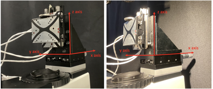
Piezo scanners are used for fast, high precision motion in one or more axes. In our project, we combine the micro PI stage controller with a moving stage on x-axis to realise three dimensional piezo scanning in our confocal microscopy.
Si PIN Photodiode
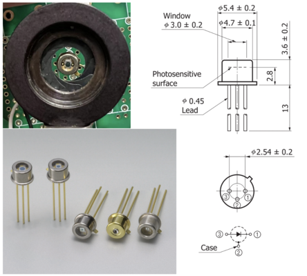
High-speed Si PIN photodiodes are designed for visible to near infrared light detection for they can efficiently convert light into an electrical current. The current is generated when photons are absorbed in the photodiode. These photodiodes provide wide-band characteristics at a low bias, making them suitable for optical communications. In this project, we choose S5973 series with a mini-lens type (S5973-01) that can be efficiently coupled with an optical fiber and a violet sensitivity enhanced type (S5973-02) ideal for violet laser detection. By combining the PIN photodiode with our adjustable optical pinhole, we get the receiving end of our confocal microscopy
Photodiode has two working modes: solar cell mode (photovoltaic mode) and photoconductive mode. Solar cell mode is otherwise called as Zero Bias Mode. When a photodiode operates in low frequency applications and ultra-level light applications, this mode is preferred. When photodiode is irradiated by a flash of light, voltage is produced. The voltage produced will have a very small dynamic range and it has a non-linear characteristic. When photodiode is configured with OP-AMP in this mode, there will be a very less variation with temperature. (sketch diagram see link below). In the photoconductive mode, photodiode will act in reverse biased condition. Cathode will be positive and anode will be negative. When the reverse voltage increases, the width of the depletion layer also increases. Due to this the response time and junction capacitance will be reduced. Comparatively this mode of operation is fast and produces electronic noise.
Arduino Uno
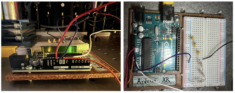
In our confocal set up, we use a 5V DC supply to inverse biase ( connect to the cathode of )the photodiode and operate it under a photoconductive mode. Some resistors are connect between photodiode anode side and ground (GND) to amplify the signal from the photodiode and convert the photo current to an readable voltage. A 47K Ohm is first adopted in the circuit, later found out that this resistor is not big enough, then we added three more 1M Ohm resistors (3.047M Ohm in total). Then three 100 nF capacitors in series (100/3 nF in total )were connected btw photodiode anode side and ground (GND) to filter out the high frequency noises of photocurrent. Finally, We use an arduino analog input pin A0 to read out the voltage at the anode side of photodiode.
Also, in our photoconductive mode, we didn't use an OP-AMP, but connecting our voltage metter directly with our photodiode's anode.
Code
* Here is an Arduino sketch to read the output voltage of the photodiode detectors.
  The output pin of the circuit is connected to analog pin 0 of the Arduino.
  The data are read every 0.025 second in this example.
  However, you can change the sampling rate by simply changing the argument of the delay() statement. *

  #define inPin0 0
  void setup(void) {
    Serial.begin(9600);
    Serial.println();
  }

 void loop(void) {
 float pinRead0 = analogRead(inPin0);
 Serial.println(pinRead0);
 /* the minimum delay allowed is about 20, correspond
 is about 20ms */}
 delay(25);
 }
Experimental process
Laser calibration
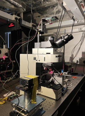
To realise the focus both on the focal plane of specimen and pinhole aperture, we built the set up shown in Figure.6. After the adjustment, we fix the height of the detector.
Measurement of coin sample
Step 1
Firstly, we managed to find the focus point within the region of 400um along z axis for each point on our coin by y-z micro PI stage controller.
Step 2
After that, we translated 100um on x-axis per step to find next focus point on z direction. We moved 10 steps in total so that the total distance along y-axis is 1000um.
Step 3
At last, we moved 100um on x-axis through tuning the spiral and measured the final set of data.
Experimental results
We tried to scan a 1mm*1mm area on the coin, and the area we focus is basically ‘E’ of word CENTS on a 50 cents Singapore dollar. Here are the scanning parameters of our experiment.

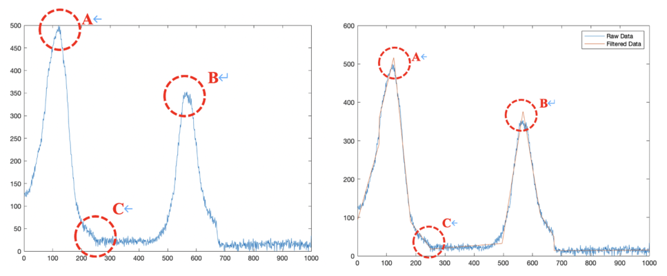
We used two piezo stage to move along y and z axis automatically, and a spiral micrometer to move the stage along x axis. Here we want to scan 10 points along x axis, 10 points along y axis and 80 points along z axis. Here is how we scan our sample: start from (x,y,z) the receiver will automatically scan 80 points when piezo moves upward along z axis (for scanning of each point piezo will take for about 85ms) and reach point (x,y,z+400), it will go pass the focused point of this certain (x,y) along the scanning of z axis, then piezo will move to point (x,y+100,z+400) and hold there for 5 seconds, then it will movie downward and reach point (x,y+100,z), it will pass through the focused point of this (x,y+400), and after that, it will move to point (x,y+200,z) and hold there still for 5 seconds. After 5 iterations of this, we will reach point (x,y+1000,z) and then we will use micrometer move the stage manually to point (x+100, y+1000,z) and repeat another 5 iterations, after moving 9 times we will reach point (x+1000, y+1000,z) finally. Figure 9 is the typical scanning pattern of two points (x,y,z+400) and (x,y+100,z+400), so we can find two corresponding maximum A&B in the plot, C is the point when piezo starts to hold still for 5 seconds.
By getting length AC and BC, we can calculate height and intensity information about each (x, y). I use MATLAB function NF.m to filter noise and Figure.9 illustrates the filtered data. Here is how we convert AC and BC to height Information. AC and BC are actually number of data points (in the spacing). We know that Arduino will sent one data to MATLAB every 25ms, so AC and BC can be converted to time. Then we know that the scanning speed of piezo stage along z axis is about 59um/s (micrometer per second), hence AC and BC can be converted to distance. Here AC and BC indicates the distance of two maximum (focused) points A and B to the upper surface, using total height 400um to subtract AC, BC will give us the height of A,B (to the lower surface).
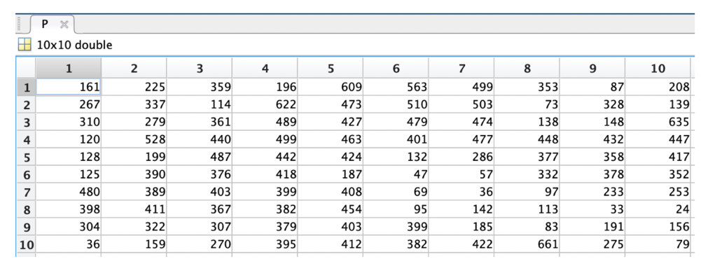
Dataphones are used to analyse the final intensity and height data. The intensity data of our sample are shown in Table 2.
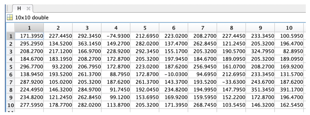
The height data of our sample are shown in Table 3.
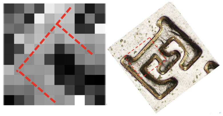
After that, we used the DrawSurf.m to draw Intensity data as illustrated in Figure 10. By comparing this result with the original "E" picture under an Optical microscope, we can find indeed this result looks like a letter "E".
Besides, we also used the DrawTopo.m to draw Intensity data and Height data as illustrated in Figure.11. Height of the brighter orange region is bigger than the darker red region. By comparing this result with the original "E" picture under an Optical microscope, we can find indeed this result also looks like a letter "E".
The final 3D results are shown in Figure 12. From that, it can be find that we have realised the three-dimensional imaging by confocal microscope.
Data Processing
Matlab Code
This SerialCom_Read.m program will build up serial communication between MATLAB and Arduino Board. The Arduino Board will read data from Photodiode and send data to MATLAB with a baud rate of 115200 (maximum of 115200 bits per second).
This program will process data and calculate the Height and Intensity Matrix
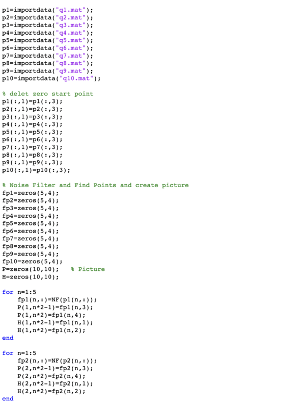

This program will filter out Noise and calculate AC, BC
This program will draw 2D image of the scanned area

This program will draw 3D profile of the scanned sample area
Discussion
In this project, we have successfully construct the confocal microscopy and further applicate that to realise the three-dimensional imaging of coin. However, some limitation should be noted. First, the long scanning time limited the scanning size of our samples, which means that we still need to figure out the program optimisation to realise the large-area scanning with shorter time. Moreover, our optical devices may juggle during the experimental process for they are not fully fixed on the console, which may introduce the noise and instrumental error to our system. That should be carefully considered if we want to get a better results from this system.
Remained Problems and Future Works
We have came across many problems in setting up this confocal microscopy. We resolved most of them, yet there are still a few remained.
To start with, for the XYZ scanner, we only have two piezo stages which can only provide automatic scanning on two directions, on the x direction we adopted a spiral micrometer which still requires manual adjustment. If automatic scanning on x direction is also achieved using an optical scanning stage, the efficiency of our laser scanning confocal microscope will be increased substantially.
Another problem is the receiving optical path which is required to refocus the reflected laser light on a spot with a certain height. However, this height is not adjustable in our setup which means that we can only change the position of our pinhole and photodiode. If height of the focused laser spot is adjustable, we can fix the pinhole and adjust the receiving optical path to refocus the beam onto the pinhole.
The Signal to Noise Ratio of our confocal microscopy is too low for a precision measurement system, with capacitors added to filter out the high frequency noise, we can only achieve SNR (20Lg(Vs/Vn)) of about 40dB. In order to achieve a higher SNR, we need to redesign photodiode's signal amplify circuit.
The piezo stage scanning and photodiode data collection is not synchronized in our system. We use different programs to control the scanning and data collection, so synchronizing them is barely possible. In order to help data receiving end distinguish different scan points and be aware of the change of location, the piezo will hold for 5 seconds after scan along z axis of each (x,y). If data collection end could be informed instantaneously when piezo stage moves its position, efficiency of the scanning could enhanced.
The last problem is that our system can't achieve quite accurate height information about the scanned area, so 3D profiling remains a problem. Some factors might be responsible for the inaccurate height information in the coin scanning. For instance, we did a 1mm*1mm scan with a resolution of only 10*10, which is quite low to depict more detailed surface information, however, higher resolution means more time consuming. Another possible factor is the imperfection in our data processing program, this might cause us found a wrong maximum point and thus gave us a wrong height of the focused point.
Except solving those problems mentioned above and increase the efficiency and precision of our confocal microscopy, there are still some functions we wish to achieve on our Laser Scanning Setup. We wish to achieving the detection of fluorescence other than reflected light, we will need an optical filter to filter out the reflected light and a much more sensitive sensor to detect and collect the fluorescence light. Longer scanning time each point might be able to offset the requirement on sensor, yet this will also decrease the efficiency of the scanning system. With the fluorescence detection ability, we will try to detect some living creatures based on this system.
Lab Location
S12-01-10/11 Nanomaterials Research Lab