A digital oscilloscope Based on MCU: Difference between revisions
| (113 intermediate revisions by the same user not shown) | |||
| Line 1: | Line 1: | ||
== Introduction == | == Introduction == | ||
We design a digital oscilloscope with STC8A8K chip as the control core, which mainly consists of two modules: hardware circuit and software program. The hardware module mainly includes OLED screen, voltage | We design a digital oscilloscope with STC8A8K chip as the control core, which mainly consists of two modules: hardware circuit and software program. The hardware module mainly includes OLED screen, voltage divider circuit, filter circuit, clock system, power supply and management module and so on. The software module mainly includes ADC sampling, OLED display, interrupt timing and some necessary data processing. its measurable bandwidth is 0-3000Hz, and measured range is 0-27V. After many tests and comparisons, the design achieves the amplification and reduction of waveform and the measurement of different frequency waveform in the experimental process, so as to achieve the desired goal. | ||
== Methodology == | == Methodology == | ||
=== Design idea=== | === Design idea=== | ||
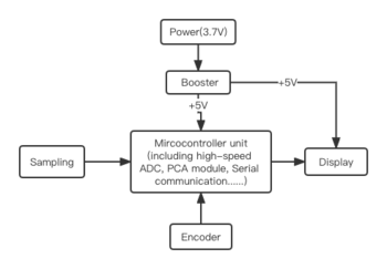
The overall circuit is shown in Figure.1. The core component of this circuit is STC8A8K64S4A12 chip, which is single clock/machine cycle microcontroller produced by STC Co. Ltd. | The overall circuit is shown in Figure.1. The core component of this circuit is STC8A8K64S4A12 chip, which is single clock/machine cycle microcontroller produced by STC Co. Ltd. We selected this microcontroller because it offers moderate performance. Rich digital peripherals and analog peripherals are provided in this microcontroller, including 4 serial ports, 5 timers, 4 sets of PCA, 8 groups of enhanced PWM and I2C, SPI, 16 channels 12 bit ADC and comparator, which can meet almost all the needs of users when designing a product. | ||
For this project, we use the serial port control send and receive a string of characters to/from an encoder, which can ensure serial data transmission between encoder and microcontroller. Also, the enhanced PMW current can light up the OLED, and the display driver IC and display peripheral supporting IC work together on the OLED display and determine its current display state. | For this project, we use the serial port control send and receive a string of characters to/from an encoder, which can ensure serial data transmission between encoder and microcontroller. Also, the enhanced PMW current can light up the OLED, and the display driver IC and display peripheral supporting IC work together on the OLED display and determine its current display state. | ||
In a digital oscilloscope, the analog signal is at the input, after amplification and preliminary filtering, goes to an analog-to-digital converter (ADC) with an external clock. Analog-to-digital conversion takes place by means of sampling.The samples are taken at specific rates and the amplitude of each sample is measured and stored. Intuitively, we know that the accuracy of the digital signal at the output depends upon the number of samples that are taken. | In a digital oscilloscope, the analog signal is at the input, after amplification and preliminary filtering, goes to an analog-to-digital converter (ADC) with an external clock. Analog-to-digital conversion takes place by means of sampling.The samples are taken at specific rates and the amplitude of each sample is measured and stored. Intuitively, we know that the accuracy of the digital signal at the output depends upon the number of samples that are taken.Inside this STC microcontroller there is a decent ADC which fulfill the requirements of high sampling rate. Using program control, the function of running and stopping ADC sampling and analysing completed sampling data in buffer, displaying and clearing waveform all can be realized. | ||
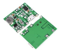
Furthermore, A 3.7V Li-ion battery supply power to the entire circuit, | Furthermore, A 3.7V Li-ion battery supply power to the entire circuit, but we want the operating voltage of microcontroller and SSD display is maintained at 5.0V.To increase the voltage, we connect the Li-ion battery and a booster in series to get a higher output voltage. The physical circuit of booster is shown in Figure.2. | ||
This digital oscilloscope was able to convert the analog input voltage to a digital voltage, write the digital data to the memory, read the digital data from the memory, convert the digital data to analog data, and display the analog data. The signal was returned via a STC microcontroller and displayed on the SSD OLED. | |||
[[File:Circuit block diagram.png|thumb|center|350px|Fig.1 Circuit block diagram]] | [[File:Circuit block diagram.png|thumb|center|350px|Fig.1 Circuit block diagram]] | ||
[[File:Adjustable Lithium Battery Charging Discharge Integrated Module.jpeg|thumb|center|250px|Fig.2 Adjustable Lithium Battery Charging Discharge Integrated Module]] | |||
===Hardware circuit module=== | ===Hardware circuit module=== | ||
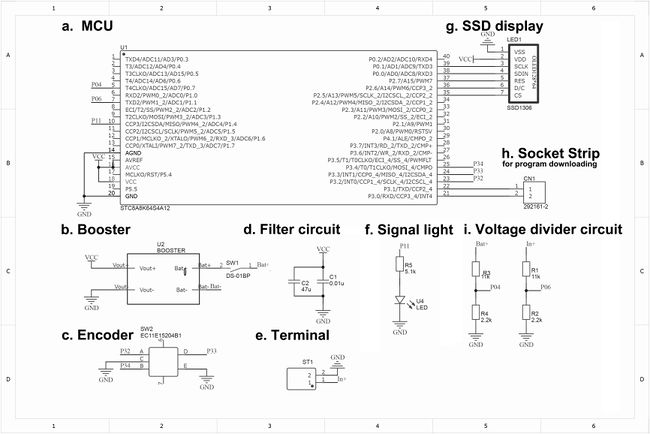
All of the key components of entire circuit is shown as below: | |||
[[File:Schematic diagram.jpeg|thumb|center|650px|Fig.3 Schematic diagram]] | |||
Each component has its own function and connection: | |||
a. Microcontroller: It is the most important part of entire circuit. Before designing the circuit, we refer to the pin definition table in the Microcontroller datasheet which shows all of the various functions available for each pin, and we confirm that every functions required for our project. | |||
b. Booster: Power module with Li-ion battery charging management and booster function. Bat+&Bat- port connect to the battery and switch. The Vout+&Vout- Port can output an adjustable voltage by rotating the potentiometer. | |||
c. Encoder(EC11): These device can generate electrical signal based on the movement of encoder, and we connect its terminal to serial port(P32,P33,P34)of microcontroller. With program control, microcontroller will receive and analyse signal sent from encoder, then we can achieve some basic operation of oscilloscope. | |||
All operations are completed by the EC11 Encoder. The input include single click, double click, long press, rotate and rotate while pressing.The details are below: | |||
*Single Click Encoder: Run/Stop sampling | |||
*Double Click Encoder: Enter Wave Scroll Mode/Parameter Mode | |||
*Long Press Encoder: Enter Settings Interface | |||
*Rotate Encoder: Adjust parameters/Scroll waveform horizontally (only available when sampling stopped) | |||
*Rotate Encoder While Pressing: Switch between options/Scroll waveform vertically (only available when sampling stopped) | |||
*Switch Auto and Manual Range: Rotate Encoder clockwise continuous to enter auto range. Rotate Encoder anticlockwise to enter manual range. | |||
d. Bypass capacitors(an electrolytic capacitor 47uF & a ceramic capacitor 10nF):These two paralleling capacitors is at the power pin of microcontroller unit. The propose of this part is to keep the input voltage more stable and filter out the voltage spikes. So it can protect the microcontroller unit when the power on. They can also filter out the low and high frequency noise respectively. | |||
e. Terminal(2 pin): It is an input of digital oscilloscope. | |||
f. Signal light(indicator): Generally, the indicator on means the sampling is running. The more important use is in Single and Normal Trigger Mode, before get into the trigger stage, pre-sampling is required. The indicator will not on during pre-sampling stage. We should not input signal until the indicator comes on. The longer time scale selected, the longer waiting time of pre-sampling. | |||
g. SSD display:In order to clearly displaying and drawing waveform in the screen, the SSD display should connect to ADC analog input channel(Pin38&39),Enhanced PWM output channel(Pin37)and PCA capture input and pulse output channel(Pin35&36)in the STC microcontroller. | |||
h. Socket strip: When a USB to TTL downloader connect to it, we can download the code to Microcontroller. | |||
i. Voltage divider circuit(a 1W 11k resistor & a 1/4w 2.2k resistor):Add two resistor in series as voltage dividing for voltage sampling of battery, which serve to convert an input voltage signal ranging from 0V to +27V to a scaled signal ranging from 0 to +5V.This is done to protect the microcontroller which requires a unipolar voltage input with a maximum of +5V volts. | |||
===Software program module=== | ===Software program module=== | ||
The code was written in C. Use Keil software to edit and compile. | |||
The complete code is [[File:main_code.doc|left]] | |||
The main function is shown below: | |||
*void main(){ | |||
/* Set ADC port P0.4, P0.6 as high-impedance */ | |||
P0M1 |= 0x50; | |||
P0M0 &= ~0x50; | |||
/* Set indicator port P1.1 as push-pull output */ | |||
P0M1 &= ~0x02; | |||
P0M0 |= 0x02; | |||
/* Set Encoder port P3.2, P3.3, P3.4 as quasi bidirectional */ | |||
P3M1 &= ~0x1C; | |||
P3M0 &= ~0x1C; | |||
/* Set OLED port P2.3, P2.4, P2.5, P2.6 as quasi bidirectional */ | |||
P2M1 &= ~0xF8; | |||
P2M0 &= ~0xF8; | |||
/* Interrupt for rotating of Encoder */ | |||
IT0 = 0; //Rising edge triggered for external interrupt 0 | |||
PX0 = 1; //High priority for external interrupt 0. Used to judge when pressing and rotating at the same time | |||
EX0 = 1; //Enable external interrupt 0 | |||
/* Interrupt for clicking of Encoder */ | |||
IT1 = 1; //Falling edge triggered for external interrupt 1 | |||
PX1 = 0; //Low priority for external interrupt 1. | |||
EX1 = 1; //Enable external interrupt 1 | |||
/* Timer 0, for updating voltage of battery */ | |||
AUXR &= 0x7F; //12T mode for timer | |||
TMOD &= 0xF0; //Set mode for timer | |||
TL0 = 0x46; //Set the timing initial value | |||
TH0 = 0x24; //Set the timing initial value | |||
TF0 = 0; //Clear TF0 | |||
ET0 = 1; //Enable timer 0 interrupt | |||
/* Enable global interrupt */ | |||
EA = 1; | |||
//UartInit(); | |||
Read_Options(); | |||
init(); | |||
OLED_Init(); | |||
OLED_SetFontWidth(6); | |||
PlotChart(); | |||
OLED_Display(); | |||
while (1) | |||
{ | |||
P_Ready = 0; | |||
/* Sampling*/ | |||
GetWaveData(); | |||
/* Enter Settings Interface */ | |||
if (InSettings) | |||
{ runWhenInSettrings(); } | |||
/* ADC Sampling Interrupt */ | |||
else if (ADCInterrupt) | |||
{ runWhenADCInterrupt(); } | |||
/* ADC Sampling Complete */ | |||
else | else | ||
{ | { runWhenADCComplete(); } | ||
}} | |||
The main program sets the initial state of the port, the encoder interrupt mode and the timer, and implements the functions by calling other functions. | |||
} | |||
== Experimental setup == | == Experimental setup == | ||
===Step 1:Preparation === | ===Step 1:Preparation === | ||
In the project, we will make a simple oscilloscope. STC8A8K64S4A12 chip has fast calculation speed, comes with ADC module and has large RAM space for sampling and OLED screen cache. In addition, AGND, AVREF, AVCC pins can improve the accuracy of sampling. So, STC8A8K64S4A12 chip was decided to be our important microcontroller module. The design idea of the circuit diagram has been clarified in previous. | |||
Material List: | Material List: | ||
* MCU: STC8A8K64S4A12(core component) | * MCU: STC8A8K64S4A12(core component) | ||
| Line 129: | Line 125: | ||
* EC11 Encoder(for controlling of oscilloscope),Toggle Switch(for power switch),2-Pin Terminal(for input of oscilloscope),LED | * EC11 Encoder(for controlling of oscilloscope),Toggle Switch(for power switch),2-Pin Terminal(for input of oscilloscope),LED | ||
* IC Socket 40-Pin,Row Pin(for installation of OLED display and programming the MCU) | * IC Socket 40-Pin,Row Pin(for installation of OLED display and programming the MCU) | ||
* 3.7V | * 3.7V Lithium-ion Battery(power source) | ||
* 5V Booster Module(power module with Li-ion charging management and boost function) | * 5V Booster Module(power module with Li-ion charging management and boost function) | ||
* USB-TTL Downloader(for downloading program to MCU) | * USB-TTL Downloader(for downloading program to MCU) | ||
| Line 135: | Line 131: | ||
===Step 2:PCB board design and layout=== | ===Step 2:PCB board design and layout=== | ||
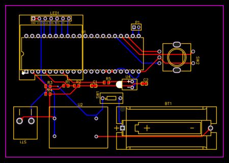
===Step 3: | PCB was deawn according to the schematic using Altium Designer. Package specifications were based on the package library provided by the software offical and other few drawn by ourselves. | ||
[[File:PCB design (Double-side circuit).jpg|thumb|center|450px|Fig.4 PCB design (Double-side circuit)]] | |||
===Step 3:Circuit soldering=== | |||
Here, we did not use a PCB but a cirucit board is to facilitate the adjustment of the circuit and the addition of components. | |||
The circuit was welted using a 350 degree soldering iron and solder according to the circuit schematic. The actual circuit we got finally is shown in figure 5. | |||
[[File:Actual soldered circuit.jpg|thumb|center|750px|Fig.5 a: Back of the actual circuit; b: Front of the actual circuit]] | |||
[[File:微信图片 20220430190245.jpg|thumb|center|450px|Fig.6 power module setting]] | |||
Then we connect battery to power management module, adjust the potentiometer to change output voltage and make the output voltage to be about +5V(Figure.6). | |||
Each interface was tested for ohms and the pin contact was good and in line with the theoretical values. Therefore, the circuit was found to be well built. | |||
===Step 4:Programming and downloading the code to microcontroller === | ===Step 4:Programming and downloading the code to microcontroller === | ||
=== | To program the microcontrollers made by ST Microelectronics you need a tool called STC-ISP(Figure.6). | ||
[[File:stcisp.jpg|thumb|center|450px|Fig.7 Interface of STC-ISP for program downloading]] | |||
[[File:usbcode.jpg|thumb|center|450px|Fig.8 Usb serial port for communication]] | |||
Connect the TXD and RXD terminals of the MCU and complete the program download by connecting to the computer via USB as shown in figure 7. The code is written in C and converted to .hex and .bin files for writing to the chip. Once the program file and EEPROM file are configured, the program can be downloaded. For the STC we use, a cold boot is required to download the program using the boot sector. | |||
During the actual operation, unexpectedly, our program could not be downloaded. | |||
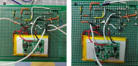
After testing, the circuit is normal, the power supply is normal, and the cold start error is suspected. However, the problem persisted after shorting P1.0 and P1.1 to ground. After checking the manual again and grounding P3.2, the program still could not be downloaded. | |||
[[File:adjustment.jpg|thumb|center|450px|Fig.9 a: Shorting P1.0 & P1.1 to ground; b: Shorting P3.2 to ground]] | |||
== Discussion == | |||
In this experiment, although there were no problems with the experimental steps, problems arose during the writing downloading phase. The main reason for choosing this chip was its ADC function and online burning function. After checking, we found that many engineers had encountered many problems during the writing downloading process. | |||
The first situation is the failure of writing downloading through the USB to serial port. The reason for this is that for some chips, a dedicated chip USB to serial port is required. The second situation is that sometimes some chips in the same batch can be programmed online, while others cannot. It may be that there are minor package differences that cause problems with this writing downloading process. | |||
There are also problems with jumping when using the chip, and sometimes the light flickers. Using direct battery power did not improve the problem, so we also ruled out a DC-DC effect. We suspected that there might also be a problem with the chip itself. We also found that this jumping problem is related to the quality of each microcontroller. | |||
== Future improvement can be done == | |||
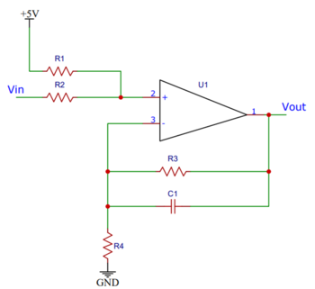
* One of the biggest design problem of this oscilloscope is the inability to measure negative voltages. Since the oscilloscope measures voltages in the range 0 V to 27 V, a shift can be made using an isotropic adder. Choose suitable resistors and capacitors in the schematic and add the adder to input part. The calculation formula is as follows. | |||
<math display='block'> | |||
\begin{align} | |||
V_{out} = \frac{V_{in}+5V}{2}*\frac{R_4+R_3}{R_4}. | |||
\end{align} | |||
</math> | |||
[[File:Amplification circuit for improvement.png|thumb|center|350px|Fig.10 Amplification circuit for improvement]] | |||
* Use a higher performance microcontroller, such as the STM32, and reduce the problems with writing downloading and jumping. | |||
* Consider accelerating the external ADC to increase the speed and add a cache mechanism. | |||
* Use a colour screen or two OLEDs, one for waveform display and one for parameter display. | |||
Throughout the project, we learned a lot more than just how to build a simple digital oscilloscope. We learned how to design a MCU circuit board. We did everything from reading and interpreting datasheets to trouble programming errors. By successfully completing these tasks and producing the functional circuit board digital oscilloscope, we were able to demonstrate fundamental levels of understanding in basic electronic techniques, digital electronics. | |||
== Reference == | |||
https://datasheetspdf.com/pdf-file/1305880/STCMCU/STC8A8K64S4A12/1 | |||
Latest revision as of 14:54, 30 April 2022
Introduction
We design a digital oscilloscope with STC8A8K chip as the control core, which mainly consists of two modules: hardware circuit and software program. The hardware module mainly includes OLED screen, voltage divider circuit, filter circuit, clock system, power supply and management module and so on. The software module mainly includes ADC sampling, OLED display, interrupt timing and some necessary data processing. its measurable bandwidth is 0-3000Hz, and measured range is 0-27V. After many tests and comparisons, the design achieves the amplification and reduction of waveform and the measurement of different frequency waveform in the experimental process, so as to achieve the desired goal.
Methodology
Design idea
The overall circuit is shown in Figure.1. The core component of this circuit is STC8A8K64S4A12 chip, which is single clock/machine cycle microcontroller produced by STC Co. Ltd. We selected this microcontroller because it offers moderate performance. Rich digital peripherals and analog peripherals are provided in this microcontroller, including 4 serial ports, 5 timers, 4 sets of PCA, 8 groups of enhanced PWM and I2C, SPI, 16 channels 12 bit ADC and comparator, which can meet almost all the needs of users when designing a product.
For this project, we use the serial port control send and receive a string of characters to/from an encoder, which can ensure serial data transmission between encoder and microcontroller. Also, the enhanced PMW current can light up the OLED, and the display driver IC and display peripheral supporting IC work together on the OLED display and determine its current display state.
In a digital oscilloscope, the analog signal is at the input, after amplification and preliminary filtering, goes to an analog-to-digital converter (ADC) with an external clock. Analog-to-digital conversion takes place by means of sampling.The samples are taken at specific rates and the amplitude of each sample is measured and stored. Intuitively, we know that the accuracy of the digital signal at the output depends upon the number of samples that are taken.Inside this STC microcontroller there is a decent ADC which fulfill the requirements of high sampling rate. Using program control, the function of running and stopping ADC sampling and analysing completed sampling data in buffer, displaying and clearing waveform all can be realized.
Furthermore, A 3.7V Li-ion battery supply power to the entire circuit, but we want the operating voltage of microcontroller and SSD display is maintained at 5.0V.To increase the voltage, we connect the Li-ion battery and a booster in series to get a higher output voltage. The physical circuit of booster is shown in Figure.2.
This digital oscilloscope was able to convert the analog input voltage to a digital voltage, write the digital data to the memory, read the digital data from the memory, convert the digital data to analog data, and display the analog data. The signal was returned via a STC microcontroller and displayed on the SSD OLED.
Hardware circuit module
All of the key components of entire circuit is shown as below:
Each component has its own function and connection: a. Microcontroller: It is the most important part of entire circuit. Before designing the circuit, we refer to the pin definition table in the Microcontroller datasheet which shows all of the various functions available for each pin, and we confirm that every functions required for our project.
b. Booster: Power module with Li-ion battery charging management and booster function. Bat+&Bat- port connect to the battery and switch. The Vout+&Vout- Port can output an adjustable voltage by rotating the potentiometer.
c. Encoder(EC11): These device can generate electrical signal based on the movement of encoder, and we connect its terminal to serial port(P32,P33,P34)of microcontroller. With program control, microcontroller will receive and analyse signal sent from encoder, then we can achieve some basic operation of oscilloscope. All operations are completed by the EC11 Encoder. The input include single click, double click, long press, rotate and rotate while pressing.The details are below:
- Single Click Encoder: Run/Stop sampling
- Double Click Encoder: Enter Wave Scroll Mode/Parameter Mode
- Long Press Encoder: Enter Settings Interface
- Rotate Encoder: Adjust parameters/Scroll waveform horizontally (only available when sampling stopped)
- Rotate Encoder While Pressing: Switch between options/Scroll waveform vertically (only available when sampling stopped)
- Switch Auto and Manual Range: Rotate Encoder clockwise continuous to enter auto range. Rotate Encoder anticlockwise to enter manual range.
d. Bypass capacitors(an electrolytic capacitor 47uF & a ceramic capacitor 10nF):These two paralleling capacitors is at the power pin of microcontroller unit. The propose of this part is to keep the input voltage more stable and filter out the voltage spikes. So it can protect the microcontroller unit when the power on. They can also filter out the low and high frequency noise respectively.
e. Terminal(2 pin): It is an input of digital oscilloscope.
f. Signal light(indicator): Generally, the indicator on means the sampling is running. The more important use is in Single and Normal Trigger Mode, before get into the trigger stage, pre-sampling is required. The indicator will not on during pre-sampling stage. We should not input signal until the indicator comes on. The longer time scale selected, the longer waiting time of pre-sampling.
g. SSD display:In order to clearly displaying and drawing waveform in the screen, the SSD display should connect to ADC analog input channel(Pin38&39),Enhanced PWM output channel(Pin37)and PCA capture input and pulse output channel(Pin35&36)in the STC microcontroller.
h. Socket strip: When a USB to TTL downloader connect to it, we can download the code to Microcontroller.
i. Voltage divider circuit(a 1W 11k resistor & a 1/4w 2.2k resistor):Add two resistor in series as voltage dividing for voltage sampling of battery, which serve to convert an input voltage signal ranging from 0V to +27V to a scaled signal ranging from 0 to +5V.This is done to protect the microcontroller which requires a unipolar voltage input with a maximum of +5V volts.
Software program module
The code was written in C. Use Keil software to edit and compile.
The complete code is File:Main code.doc
The main function is shown below:
*void main(){
   /* Set ADC port P0.4, P0.6 as high-impedance */
   P0M1 |= 0x50;
   P0M0 &= ~0x50;
   /* Set indicator port P1.1 as push-pull output */
   P0M1 &= ~0x02;
   P0M0 |= 0x02;
   /* Set Encoder port P3.2, P3.3, P3.4 as quasi bidirectional */
   P3M1 &= ~0x1C;
   P3M0 &= ~0x1C;
   /* Set OLED port P2.3, P2.4, P2.5, P2.6 as quasi bidirectional */
   P2M1 &= ~0xF8;
   P2M0 &= ~0xF8;
   /* Interrupt for rotating of Encoder */
   IT0 = 0; //Rising edge triggered for external interrupt 0
   PX0 = 1; //High priority for external interrupt 0. Used to judge when pressing and rotating at the same time
   EX0 = 1; //Enable external interrupt 0
   /* Interrupt for clicking of Encoder */
   IT1 = 1; //Falling edge triggered for external interrupt 1
   PX1 = 0; //Low priority for external interrupt 1.
   EX1 = 1; //Enable external interrupt 1
   /* Timer 0, for updating voltage of battery */
   AUXR &= 0x7F; //12T mode for timer
   TMOD &= 0xF0; //Set mode for timer
   TL0 = 0x46;   //Set the timing initial value
   TH0 = 0x24;   //Set the timing initial value
   TF0 = 0;      //Clear TF0
   ET0 = 1;      //Enable timer 0 interrupt
   /* Enable global interrupt */
   EA = 1;
   //UartInit();
   Read_Options();
   init();
   OLED_Init();
   OLED_SetFontWidth(6);
   PlotChart();
   OLED_Display();
   while (1)
   {
       P_Ready = 0;
       /* Sampling*/
       GetWaveData();
       /* Enter Settings Interface */
       if (InSettings)
       {            runWhenInSettrings();        }
       /* ADC Sampling Interrupt */
       else if (ADCInterrupt)
       {            runWhenADCInterrupt();        }
       /* ADC Sampling Complete */
       else
       {            runWhenADCComplete();        }
   }}
The main program sets the initial state of the port, the encoder interrupt mode and the timer, and implements the functions by calling other functions.
Experimental setup
Step 1:Preparation
In the project, we will make a simple oscilloscope. STC8A8K64S4A12 chip has fast calculation speed, comes with ADC module and has large RAM space for sampling and OLED screen cache. In addition, AGND, AVREF, AVCC pins can improve the accuracy of sampling. So, STC8A8K64S4A12 chip was decided to be our important microcontroller module. The design idea of the circuit diagram has been clarified in previous.
Material List:
- MCU: STC8A8K64S4A12(core component)
- Display: SSD OLED with 7-Pin SPI Interface
- Resistor:1W 11k&1/4W 2.2k(for voltage division), 1/4W 11k(for current limiting) ,5k
- Capacitor:47uF, 0.01uF(for wave filtering)
- EC11 Encoder(for controlling of oscilloscope),Toggle Switch(for power switch),2-Pin Terminal(for input of oscilloscope),LED
- IC Socket 40-Pin,Row Pin(for installation of OLED display and programming the MCU)
- 3.7V Lithium-ion Battery(power source)
- 5V Booster Module(power module with Li-ion charging management and boost function)
- USB-TTL Downloader(for downloading program to MCU)
- Circuit Board
Step 2:PCB board design and layout
PCB was deawn according to the schematic using Altium Designer. Package specifications were based on the package library provided by the software offical and other few drawn by ourselves.
Step 3:Circuit soldering
Here, we did not use a PCB but a cirucit board is to facilitate the adjustment of the circuit and the addition of components. The circuit was welted using a 350 degree soldering iron and solder according to the circuit schematic. The actual circuit we got finally is shown in figure 5.

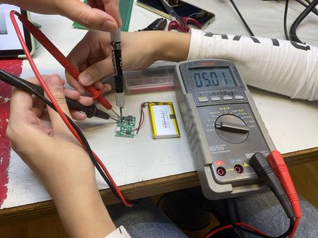
Then we connect battery to power management module, adjust the potentiometer to change output voltage and make the output voltage to be about +5V(Figure.6).
Each interface was tested for ohms and the pin contact was good and in line with the theoretical values. Therefore, the circuit was found to be well built.
Step 4:Programming and downloading the code to microcontroller
To program the microcontrollers made by ST Microelectronics you need a tool called STC-ISP(Figure.6).
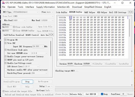
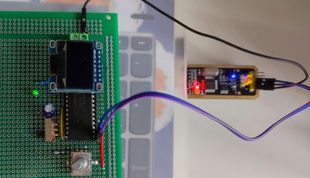
Connect the TXD and RXD terminals of the MCU and complete the program download by connecting to the computer via USB as shown in figure 7. The code is written in C and converted to .hex and .bin files for writing to the chip. Once the program file and EEPROM file are configured, the program can be downloaded. For the STC we use, a cold boot is required to download the program using the boot sector.
During the actual operation, unexpectedly, our program could not be downloaded.
After testing, the circuit is normal, the power supply is normal, and the cold start error is suspected. However, the problem persisted after shorting P1.0 and P1.1 to ground. After checking the manual again and grounding P3.2, the program still could not be downloaded.
Discussion
In this experiment, although there were no problems with the experimental steps, problems arose during the writing downloading phase. The main reason for choosing this chip was its ADC function and online burning function. After checking, we found that many engineers had encountered many problems during the writing downloading process.
The first situation is the failure of writing downloading through the USB to serial port. The reason for this is that for some chips, a dedicated chip USB to serial port is required. The second situation is that sometimes some chips in the same batch can be programmed online, while others cannot. It may be that there are minor package differences that cause problems with this writing downloading process.
There are also problems with jumping when using the chip, and sometimes the light flickers. Using direct battery power did not improve the problem, so we also ruled out a DC-DC effect. We suspected that there might also be a problem with the chip itself. We also found that this jumping problem is related to the quality of each microcontroller.
Future improvement can be done
- One of the biggest design problem of this oscilloscope is the inability to measure negative voltages. Since the oscilloscope measures voltages in the range 0 V to 27 V, a shift can be made using an isotropic adder. Choose suitable resistors and capacitors in the schematic and add the adder to input part. The calculation formula is as follows.
- Use a higher performance microcontroller, such as the STM32, and reduce the problems with writing downloading and jumping.
- Consider accelerating the external ADC to increase the speed and add a cache mechanism.
- Use a colour screen or two OLEDs, one for waveform display and one for parameter display.
Throughout the project, we learned a lot more than just how to build a simple digital oscilloscope. We learned how to design a MCU circuit board. We did everything from reading and interpreting datasheets to trouble programming errors. By successfully completing these tasks and producing the functional circuit board digital oscilloscope, we were able to demonstrate fundamental levels of understanding in basic electronic techniques, digital electronics.
Reference
https://datasheetspdf.com/pdf-file/1305880/STCMCU/STC8A8K64S4A12/1
