Confocal Microscopy: Difference between revisions
| Line 11: | Line 11: | ||
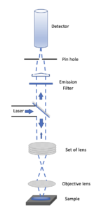
[[File: Fig 2 .png|x300px|right|thumb|Figure 1. Schematic of confocal microscopy]] | [[File: Fig 2 .png|x300px|right|thumb|Figure 1. Schematic of confocal microscopy]] | ||
The method of image formation in a confocal microscope is fundamentally different from that in a conventional traditional [https://en.wikipedia.org/wiki/Fluorescence_microscope fluorescence microscope ], where the entire specimen is subjected to intense illumination from an incoherent lam, and resulting image of secondary fluorescence emission can be viewed directly by eye or detector. In contrast, the illumination in a confocal microscope is achieved by scanning focused beam from laser and across the specimen. | |||
The confocal principle | The confocal principle is diagrammatically presented in Figure 1. Coherent light emitted by the laser system (excitation source) pass through a low-pass filter that is situated in a conjugate plane (confocal) with a scanning point on the specimen and a pinhole aperture positioned in front of the detector (Si PIN photodiode). As the laser is reflected by a dichromatic mirror and scanned across the specimen in a defined focal plane, secondary fluorescence emitted from points on the specimen pass back through the dichromatic mirror and are focused as a confocal point at the pinhole aperture. | ||
==Set up== | ==Set up== | ||
Revision as of 12:29, 26 April 2022
Introduction
A Confocal Microscopy is an optical imaging technique for increasing optical resolution and contrast of a micrograph. It uses pinhole to block out all out of focus light to enhance optical resolution, very different from traditional wide-field fluorescence microscopes. To offset the block of out of focus lights, the light intensity is detected by a photomultiplier tube or avalanche photodiode, which transforms the light signal into an electrical one. We will try to build a Setup like this to enhance optical resolution and maybe get profile information about the sample.
Team Members
Wang Tingyu, Xue Rui, Yang Hengxing
Principles of confocal microscopy

The method of image formation in a confocal microscope is fundamentally different from that in a conventional traditional fluorescence microscope , where the entire specimen is subjected to intense illumination from an incoherent lam, and resulting image of secondary fluorescence emission can be viewed directly by eye or detector. In contrast, the illumination in a confocal microscope is achieved by scanning focused beam from laser and across the specimen.
The confocal principle is diagrammatically presented in Figure 1. Coherent light emitted by the laser system (excitation source) pass through a low-pass filter that is situated in a conjugate plane (confocal) with a scanning point on the specimen and a pinhole aperture positioned in front of the detector (Si PIN photodiode). As the laser is reflected by a dichromatic mirror and scanned across the specimen in a defined focal plane, secondary fluorescence emitted from points on the specimen pass back through the dichromatic mirror and are focused as a confocal point at the pinhole aperture.
Set up

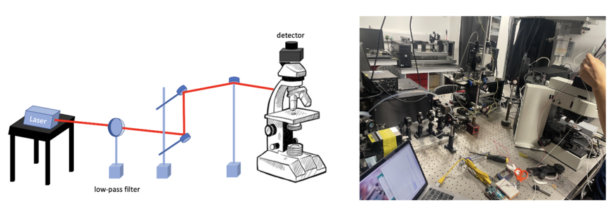
The confocal fluorescence microscope consists of multiple laser excitation sources, a scan head with optical and electronic components, electronic detector (Si PIN photodiode), and a computer for acquisition, processing, analysis, and display of images.
Lab Location
S12-01-10/11 Nanomaterials Research Lab