A digital oscilloscope Based on MCU: Difference between revisions
| Line 56: | Line 56: | ||
===Step 4:Programming and downloading the code to microcontroller === | ===Step 4:Programming and downloading the code to microcontroller === | ||
[[File:stcisp.jpg|thumb|left|450px|Fig.6 Interface of STC-ISP for program downloading]] | [[File:stcisp.jpg|thumb|left|450px|Fig.6 Interface of STC-ISP for program downloading]] [[File:usbcode.jpg|thumb|right|450px|Fig.7 Usb serial port for communication]] | ||
===Step 5:Test and measurement=== | ===Step 5:Test and measurement=== | ||
Revision as of 07:46, 30 April 2022
Introduction
We design a digital oscilloscope with STC8A8K chip as the control core, which mainly consists of two modules: hardware circuit and software program. The hardware module mainly includes OLED screen, voltage divider circuit, filter circuit, clock system, power supply and management module and so on. The software module mainly includes ADC sampling, OLED display, interrupt timing and some necessary data processing. its measurable bandwidth is 0-3000Hz, and measured range is 0-30V. After many tests and comparisons, the design achieves the amplification and reduction of waveform and the measurement of different frequency waveform in the experimental process, so as to achieve the desired goal.
Methodology
Design idea
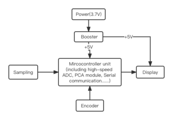
The overall circuit is shown in Figure.1. The core component of this circuit is STC8A8K64S4A12 chip, which is single clock/machine cycle microcontroller produced by STC Co. Ltd. It is a new generation of microcontroller with wide voltage range, high speed, high reliability, low power and super strong anti-interference. Rich digital peripherals and analog peripherals are provided in this microcontroller, including 4 serial ports, 5 timers, 4 sets of PCA, 8 groups of enhanced PWM and I2C, SPI, 16 channels 12 bit ADC and comparator, which can meet almost all the needs of users when designing a product.
For this project, we use the serial port control send and receive a string of characters to/from an encoder, which can ensure serial data transmission between encoder and microcontroller. Also, the enhanced PMW current can light up the OLED, and the display driver IC and display peripheral supporting IC work together on the OLED display and determine its current display state.
In a digital oscilloscope, the analog signal is at the input, after amplification and preliminary filtering, goes to an analog-to-digital converter (ADC) with an external clock. Analog-to-digital conversion takes place by means of sampling.The samples are taken at specific rates and the amplitude of each sample is measured and stored. Intuitively, we know that the accuracy of the digital signal at the output depends upon the number of samples that are taken.The STC microcontroller provide high-accuracy and high-speed ADC which fulfill the requirements of high sampling rate. Using program control, the function of running and stopping ADC sampling and analysing completed sampling data in buffer, displaying and clearing waveform all can be realized.
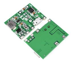
Furthermore, A 3.7V Li-ion battery supply power to the entire circuit, but we want the operating voltage of microcontroller and SSD display is maintained at 5.0V.To increase the voltage, we connect the Li-ion battery and a booster in series to get a higher output voltage. The physical circuit of booster is shown in Figure.2.
This digital oscilloscope was able to convert the analog input voltage to a digital voltage, write the digital data to the memory, read the digital data from the memory, convert the digital data to analog data, and display the analog data. The signal was returned via a STC microcontroller and displayed on the SSD OLED.
Hardware circuit module
The Hardware circuit is mainly divided into following parts and respective function are listed as follows:
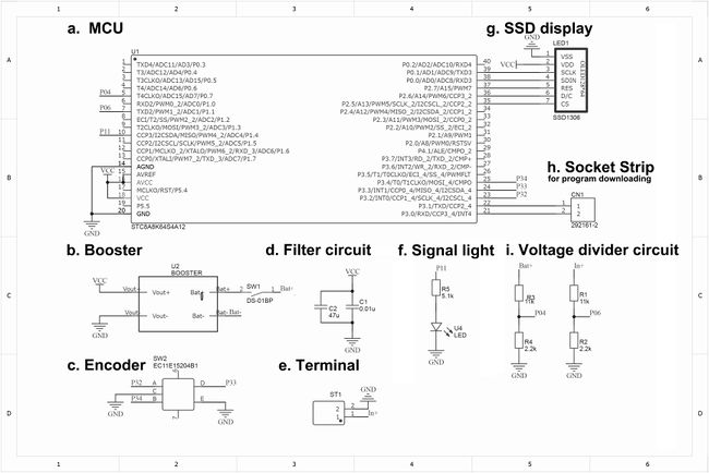
A. Decoupling capacitors(a electrolytic capacitor 47uF & a ceramic capacitor 10nF):These two capacitors is at the power pin of microcontroller unit. The propose of this part is to keep the input voltage more stable and filter out the voltage spikes. So it can protect the microcontroller unit when the power on. They can also filter out the low and high frequency noise respectively.
B. Voltage divider circuit(a 1W 11k resistor & a 1/4w 2.2k resistor): which serve to convert an input voltage signal ranging from 0V to +30V to a scaled signal ranging from 0 to +5V.This is done to protect the ADC which requires a unipolar voltage input with a maximum of +5V volts.
b. Booster: VIN+Port input , BAT+port can output 5.0V to charger 3.7V Li-ion battery. The OUT+Port can output an adjustable voltage
Software program module
Experimental setup
Step 1:Preparation
In the project, we will make a simple oscilloscope. STC8A8K64S4A12 chip has fast calculation speed, comes with ADC module and has large RAM space for sampling and OLED screen cache. In addition, AGND, AVREF, AVCC pins can improve the accuracy of sampling. So, STC8A8K64S4A12 chip was decided to be our important microcontroller module. The design idea of the circuit diagram has been clarified in previous.
Material List:
- MCU: STC8A8K64S4A12(core component)
- Display: SSD OLED with 7-Pin SPI Interface
- Resistor:1W 11k&1/4W 2.2k(for voltage division), 1/4W 11k(for current limiting) ,5k
- Capacitor:47uF, 0.01uF(for wave filtering)
- EC11 Encoder(for controlling of oscilloscope),Toggle Switch(for power switch),2-Pin Terminal(for input of oscilloscope),LED
- IC Socket 40-Pin,Row Pin(for installation of OLED display and programming the MCU)
- 3.7V Li-ion Battery(power source)
- 5V Booster Module(power module with Li-ion charging management and boost function)
- USB-TTL Downloader(for downloading program to MCU)
- Circuit Board
Step 2:PCB board design and layout
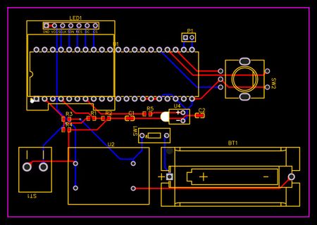
PCB was deawn according to the schematic using Altium Designer. Package specifications were based on the package library provided by the software offical and other few drawn by ourselves.
Step 3:Circuit soldering
The circuit was welted using a 350 degree soldering iron and solder according to the circuit schematic.

Each interface was tested for ohms and the pin contact was good and in line with the theoretical values. Therefore, the circuit was found to be well built.
Step 4:Programming and downloading the code to microcontroller
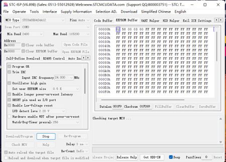
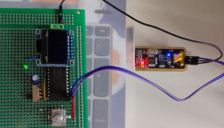
Step 5:Test and measurement
Discussion
Throughout the project, we learned a lot more than just how to build a breadboard digital oscilloscope. We learned how to design a breadboard digital oscilloscope. We did everything from reading and interpreting data sheets to trouble programming errors. By successfully completing these tasks and producing the functional breadboard digital oscilloscope we were able to demonstrate fundamental levels of understanding in basic electronic techniques, digital electronics, data acquisition, and data analysis.